Design overview
preferences
our advantage
design capability
design cycle
design services
products show
after-sales service
Overview of PCB design
professional PCB design concept, excellent PCB LAYOUT team, strict design process to the customer to
for high efficiency and quality of service. Customers only need to provide basic schematic and specification data,
is designed from the PCB board and the board patch, and we provide a one-stop solution.
speed up your product research and development and promote the rapid listing of new products,
fully grasps the market opportunity to win more economic benefits.

- 1Senior PCB design engineer, per capita 10 years, more than 80 precision board design experience.
- 2More than 800 cooperative customers
- 3Provide a multi - person parallel 7*24 - hour service that can be delivered at the fastest time of the day
- 4Packaging engineer, Layout engineer, EMI engineer, EMC engineer, professional cornerstone

| Tallest layer number | 40 layer | Minimum line width | 2mil (HDI) |
| Maximum PIN number | 60000 | Minimum line distance | 2mil (HDI) |
| Minimum BGA spacing | 0.20mm | Maximum BGA-PIN number | 2500 |
| Maximum speed signal | 12G (differential signal) | The highest price HDI | Arbitrary layer interaction (ELIC) |


| single board PIN number | Design delivery date (working day) |
| 1000within | 3-5days |
| 2000-3000 | 5-7days |
| 4000-5000 | 8-12days |
| 6000-7000 | 12-15days |
| 8000-9000 | 15-18days |
| 10000-13000 | 18-20days |
| 14000-15000 | 20-22days |
| 16000-20000 | 22-30days |
PCB Layout Design experience

-

Valuation release
-

Audit quotation
-

Payment confirmation
-

Start design
-
 Multiple confirmation
-

Finish uploading
-

Customer Download
-

Feedback audit
-
Customers need to provide information
Schematic diagram (DSN or PowerLogic), net table, encapsulation, structure diagram (DXF), device data and design requirements for new building
-
Layout and wiring review
According to the design specification, design guidance, customer design requirements and related CHECKLIST. After the project was started, our engineer carried out the schematic diagram DRC inspection, the structure check and other electrical design requirements, and the first time to feedback the EQ record to the customer.
-
Customer layout confirmation
Provide layout files, structure files for customer layout review, customers confirm the layout rationality, stacking scheme, impedance scheme, structure, package, and confirm the wiring parameters.
-
Design data output
PCB source document, Gerber file, assembly file, steel net file, structure file and so on. After the completion of PCB Layout design, our engineers conduct mutual inspection, including DFM inspection, QA inspection, EMC inspection, customer confirmation OK, Gerber and other production documents

- 1Free of charge for customers to provide PCB package construction (customer provided device DataSheet)
- 2Free of charge for customers to provide PCB impedance calculation, stack design, QA inspection, process inspection, EMC inspection.
- 3The design includes high speed, high frequency, high power, analog, digital and mode mixing, HDI, FPC and other design types.
- 4Support schematic diagram and PCB software format:Cadence,Mentor ee,Mentor pads,Altium,AD。
- 5The company's powerful R&D engineer team makes technical support to assist customers and Layout engineers in schematic analysis and PCB design, eliminating electrical design errors, and ensuring the quality and reliability of the design.
- 6Door-to-door service, according to the confidentiality of the customer's products and the talent dispatch service provided by the shortage of human resources, our engineers can make design services on the client side, which is efficient and efficient.


4 layer slab main board
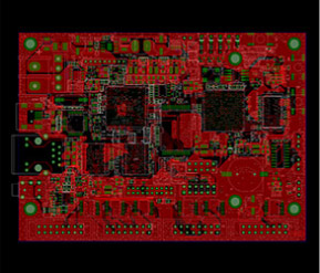
6 layer large screen display main board
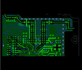
Signal processing of router board antenna
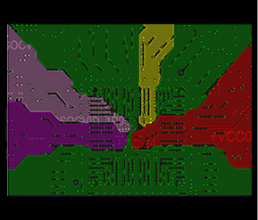
Power supply processing
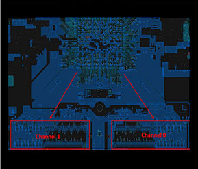
Intel platform

6 layer network main board
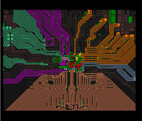
Power supply processing
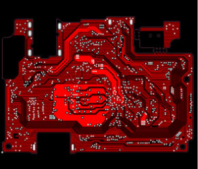
6 layer network main board
- After-sale service
- 1.Change the workload within 1 days for free.
2.Dealing with technical problems at any time
3.Coordination with hardware debugging
- Disclaimer
- 1.We are not responsible for the delay due to incomplete information.
2.Our department is not responsible for the final loss due to the information provided by the customer.
3.We are not responsible for the design of the final data due to the failure of the customer's inspection confirmation.
4.Due to the untimely confirmation of the customer, we have the right to postpone the date of the project


